High Quality, Epitaxial Thin-Films and Devices:
- Custom Wafers: Epitaxial thin-films and device structures, including III-nitrides, III-oxides, metal-nitrides, metal-oxides, graded and modulated index alloys, n-type, p-type, or undoped.
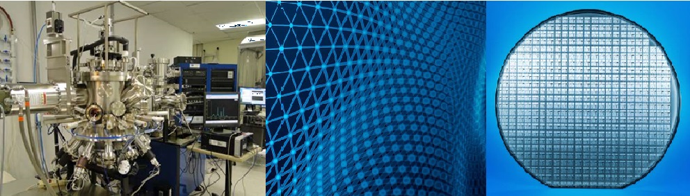
- Substrates: A12O3 , Si, SiC, ZnO, glass and others, up to 8″ diameter
- Deposition techniques: Plasma-assisted MBE, e-beam, PLD, ALD, and reactive magnetron sputtering, room temperature to >1100°C.
- Available characterization: In-situ RHEED, cathodoluminescence, optical reflectometry/pyrometery, ellipsometry, and post-deposition XRD, AFM, SEM, and dc and RF device measurements.
- Device structures: (Al,In)GaN photocathodes, Schottky and p-i-n photodiodes, Al(Ga)N/GaN HEMTs and superlattice structures, and other III-nitride and III-oxide based devices.
- R&D capabilities (open to joint collaborations): Design of experiments, device structures and thin-film deposition equipment, and preparation of related project plans and proposals.
Examples of III-Nitride Wafer Specifications:
| Epitaxial layers | GaN, AlGaN, InGaN, etc. |
| 4″ Wafer uniformity GaN/A12O3 | < 4% |
| X-Ray FWHM GaN/A12O3 | < 3 arc min |
| Intentional n-type doping (Si) | 1016 to 1020 cm-3 |
| Intentional p-type doping (Mg) | 1017 to 1019 cm-3 |
| Insulating Buffer Donor Density | Nd < 1016 cm-3 |
| AlGaN/GaN HEMT Hall Mobility* | > 1500 cm2 /Vs (300K) |
| Low temperature Hall Mobility * | > 4000 cm2 /Vs (77K) |
| Substrates | Sapphire, SiC, Si |
* HEMT characteristics depend on buffer and active layer structure.